The steps involved in a typical photomask writing and development process using a positive resist are detailed below.
A brief description of each step follows:
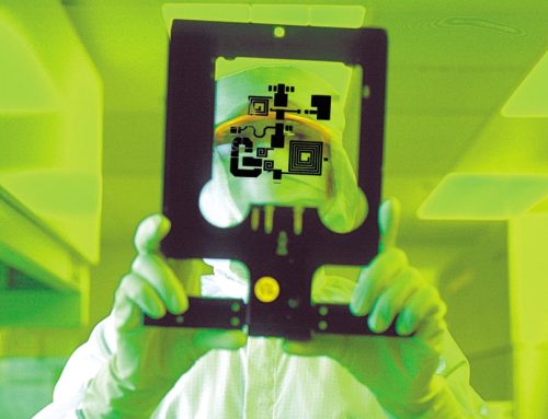
- The process begins with a verified design drawn using CAD design tool software.
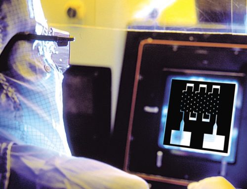
- Mask data preparation software converts or “fractures” the data into a format that describes the pattern to an optical, laser or electron beam (e-beam) writer (pattern generator).
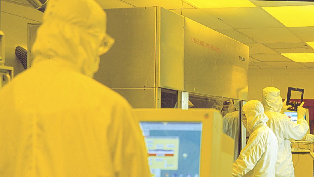
- The pattern generator writes the pattern on top of a photomask blank by exposing the photo resist to UV light, laser or electron beam.
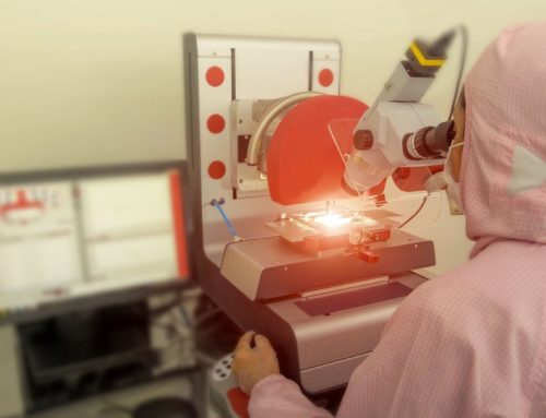
- After exposure, the photo resist is developed, which clears away the sensitized photo resist and uncovers the underlying metallization coating only where desired.
- The unprotected metallization coating is then etched (chemically removed), while the areas still protected by the remaining photo resist are left in place.
- After etching, the remaining photo resist is removed, leaving the circuit image as transparent areas in the otherwise opaque coating film.
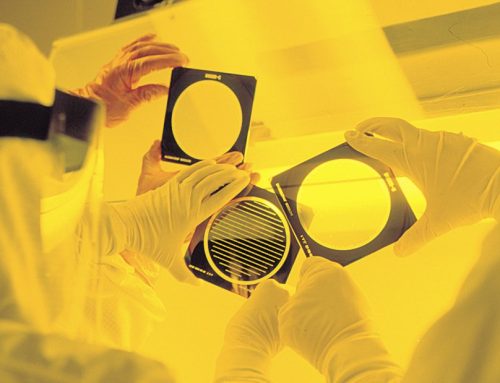
- Photomasks for wafer steppers or projection aligners can be protected against contamination by mounting a pellicle (thin, transparent membrane) that seals off the mask surface from airborne particulates and other forms of contamination. The membrane is mounted onto a metal frame (usually anodized Aluminum), called a standoff, which is securely attached to the photomask. Generally, the pellicle is attached only onto the coated side of masks. Some aligners and wafer steppers call for both sides of the reticle/photomask to be pellicalized.
PROCESS PATTERN DESIGN
The mask pattern may be designed using any number of CAD tool programs. The specific type of CAD program used to create the pattern design is of little or no importance to the maskmaker or to the mask making process. The most important consideration is that whichever CAD tool program is used, it should have the ability to output data into one of the intermediate data formats that can be accepted and converted by the mask-maker.