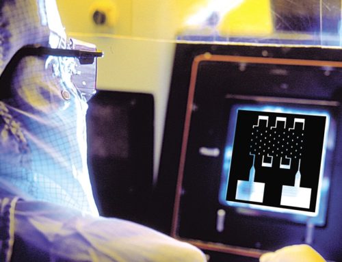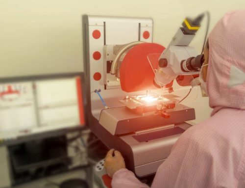
Photomasks must be of the highest quality and must meet a wide variety of customer specifications.
The photomask quality requirements are usually defined by each individual customer. The feature sizes and tolerances indicated here are of a general nature and are what would typically be available from commercial photomask suppliers on e-beam generated photomasks or direct-write laser generated photomasks. While each photomask specification is unique, there are sets of conditions that are important to most customers. These include:
- Mask flatness – expressed in microns per inch across the diagonal of the substrate. Standard = 15 (per inch across the diagonal), tightened = 5, master grade = 2.
Registration (absolute) – expressed in microns as a comparison to a NIST grid. Standard = +/- 0.75, tightened = +/- 0.5, master grade = +/- 0.25, tightest = +/-0.15. Tighter tolerances usually result in higher photomask costs.
- Registration (layer to layer) – expressed in microns as a comparison of one photomask in a mask set to any other photomask in that same mask set. Standard = +/- 0.5, tightened = +/- 0.25, tightest = +/-0.15. Tighter tolerances usually result in higher photomask costs.
- CRITICAL DIMENSION (CD) – expressed in microns. Often times the smallest feature is designated to be the “critical dimension” (CD). The maskmaker uses the CD to monitor the exposure, developing and etching. Too much or too little exposure, while developing or etching can change the final feature size from what it was on the original data file. The smallest feature is desirable to use as a CD, because changes will occur faster and more dramatically than they will on larger features. The maskmaker monitors the CD throughout the process knowing that if the CD feature is controlled within the specified tolerance, all other feature sizes will be within specification. Smaller CD feature sizes usually result in higher photomask costs.
- Minimum feature size – expressed in microns. The smallest feature found anywhere on the photomask. Often times the smallest feature may also be the critical dimension (CD) (see CRITICAL DIMENSION, above). Standard = 5.0 Tightened = 2.0 Smallest available = 0.5. Features smaller than 0.5 can be achieved through the use of reduction steppers, high-end direct-write e-beam, and direct write focused ion beam (FIB). Smaller feature sizes usually result in higher photomask costs.
- Critical Dimension / Feature size tolerance – expressed in microns. Standard = +/- 0.5, Tightened = +/- 0.25 Tightest = +/- 0.05. Tighter tolerances usually result in higher photomask costs.
- Feature size uniformity – expressed in microns. Indicates the maximum allowable variance in the CD or minimum feature size throughout the entire pattern area of the photomask. Standard = +/- 0.25, Tightened = +/- 0.2 Tightest = +/- 0.15.
- Defect size – expressed in microns. Indicates the size a hard defect (chrome spot, pinhole, scratch, protrusion, intrusion) must be before it is classified and counted as a defect. Standard = 5.0, Tightened = 2.0, Tightest = 0.5.
- Defect density – expressed in number per square inch, number per square centimeter, or number per entire pattern area. Defect density tells the maskmaker how many defects are allowable within a pre-defined area of those defects exceeding the size indicated in Defect size (above). Standard = zero > 5.0, tightened = zero > 2.0, tightest = 0 > 0.5.
- Catastrophic defect – expressed in microns. The physical size of a hard defect (chrome spot, pinhole, scratch, protrusion, intrusion), the presence of which defects the entire photomask.
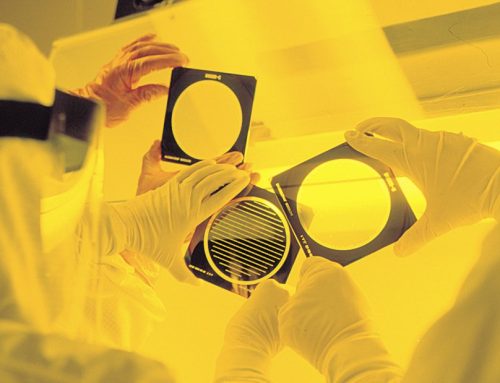
- Cleanliness – Photomasks must be extremely clean. Any contaminants on the photomask may cause defects on the wafer. Photomasks must be free of any particulates (soft defects) at the time they are packaged for shipment.
- Mask Polarity – Polarity defines the tone of certain regions of the photomask. Polarity may be expressed in terms such as “light field” or dark field” or “clear field” or “opaque field”. As previously mentioned, these polarity designations are open to interpretation and not specific enough to be reliable. Dark and clear regions of the photomask should be very specifically indicated whenever possible. This can be achieved by marking regions of a paper plot of the device as “dark or clear”. An alternate method would be to indicate that the “drawn or digitized” areas of the customer-supplied data are to be either “dark or clear”.
- Mask Parity – Parity defines the reading of the mask (mirrored or non-mirrored). A number of terminologies are used to define this. One of these is “right reading base”, which indicates that the mask pattern and accompanying text will read correctly (non-mirrored) when the mask is viewed looking at the glass side (non- metallized side). The opposite statement, “wrong reading base” is also acceptable and would indicate that the mask pattern and accompanying text will read incorrectly (mirrored) when the mask is viewed looking at the glass side (non-metallized side). Another common terminology is “right reading chrome” which indicates that the mask pattern and accompanying text will read correctly (non-mirrored) when the mask is viewed looking at the metallized side. The opposite statement, “wrong reading chrome” which indicates that the mask pattern and accompanying text will read incorrectly (mirrored) when the mask is viewed looking at the metallized side is also an acceptable way of indicating parity.
Parity can be confusing to both the designer and the maskmaker, so it is important that it is clearly communicated to avoid costly errors and delays.
A good rule of thumb is to consider the end use of the photomask. If the photomask is to be used as an intermediate tool to transfer the image to another substrate it will usually be “right reading base” or “wrong reading chrome”. The reason for this is that, typically, the data designer’s intent is for their pattern to look the same when viewing their substrate as it does when viewing the data on their CAD system. Because the pattern data “mirrors” each time a new generation is created, the mask parity must be opposite of the desired reading on the substrate. Conversely, if the photomask itself is the end product (such as an eyepiece reticle or a calibration standard), the likelihood is that it should be “right reading chrome” or “wrong reading base”. These rules are intended as a guide, but they are not true 100% of the time. The designer and the maskmaker should always make sure that the parity is understood and clearly communicated.
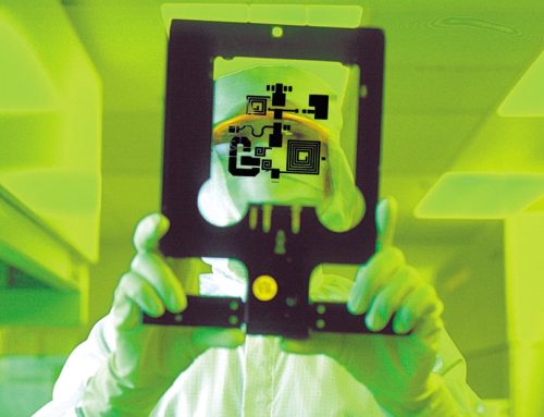
- Mask Titling – Photomasks typically include some titles that are readable to the unaided eye. The purpose of these titles is to identify the photomask. Several types of information are usually included in the mask title. They are “customer name”, “customer device number or part number”, “customer layer number”, “date of manufacture”, “name of the photomask supplier”, “photomask supplier’s internal tracking or reference number”. Other information can be included in the titles if desired.
- Mask Packaging – Photomasks are packaged prior to shipment. The most common type of packaging is a container called a “compact”. Compacts are plastic boxes, which are manufactured in clean-room environments and then delivered to the maskmaker in a manner that keeps them clean until they are ready for use. The plastic used to manufacture the compacts may be transparent or opaque, but in all cases they must have acceptable anti-static characteristics. The final photomask, inspected and clean, is placed into the compact and the compact is snapped shut. A label with the appropriate information (customer name, device number, part number, layer number, maskmaker’s internal tracking number, date, CD measurements, etc.) is affixed to one surface of the compact. The labeled compact containing the photomask is inserted into an anti-static plastic bag and sealed (permanent seal such as heat seal, or temporary seal such as zip-lock).
The sizes of photomasks can range from 2.5 inches square to 24 inches square or even larger for some flat panel display applications. Certain types of wafer steppers use a 7.25 inches round reticle/photomask. The customer specifies the thickness of the photomasks, and available thicknesses range from 40 mils (1,016 microns/1.016mm) to 250 mils (6350 microns/6.35mm).

Chrome and FeO2 photomasks