- Alignment Mark, Keys: An image selectively placed within or outside an array for either testing or aligning or both.
- AR: Anti-reflective layer.
- Array: The entire pattern area of the photomask, including all primary and secondary circuit patterns.
- Border data: Patterns that appear in the border area of photo tooling; these patterns may include tooling holes bulls-eyes, identification, test patterns, and registration marks.
- Blank: A glass substrate (quartz or soda lime) which has been coated with chrome and photo resist, but which has not yet been exposed. This is the maskmaker’s raw material.
- CAD: CAD (Computer Aided Design) data that describes the patterns to be written on the pattern generators. The data is created using software for the design of electronic circuits. Common data formats created with CAD software are GDSII and DXF/DWG.
- C.D.: The C.D. is the critical dimension. The critical dimension is a small feature on the pattern data that is designated by the designer / end-user and assigned a plus/minus tolerance. The maskmaker uses the C.D. to monitor process and exposure parameters and to insure that the final photomask meets the customer’s size specifications.
- CDC: Critical Dimension Correction. A set of functions that help compensate for effects that cause the dimensions in the exposed pattern to differ from the dimension in the pattern input data. There are several sources for such aberrations including stray light, etch undercut, chemical loading in dry etch, proximity to other pattern structures and writing structures that are small compared with the exposure beam dimension. This correction is performed by the Mask Shop.
- Classify: The process in which an inspection operator, using magnification, views defects found by an automatic inspection system. Each defect is “classified” by the operator as either hard defects, which may be repaired, or soft defects, which can be removed by cleaning.
- Clear field/Light field: A terminology used to indicate the tone of pattern or background. These terminologies are open for interpretation, and therefore terminologies that directly indicate the tone of either digitized (drawn) data, or non-digitized area (background) should be used whenever possible.
- Closure Check: The closure check is a pattern that is written onto a photomask that allows a visual check to insure that a machine or data error did not occur during the write process. A pattern, such as a square ring is written at the beginning of the write process, and a second pattern, such as a small square positioned in the center of the ring, is written at the very end of the write process. An operator may view and measure the closure check pattern to determine if the write process was compromised.
- Compact: A dust free, anti-static plastic container, which holds a single photomask. Compacts are used to ship and store photomasks.
- Compensation: Changes made in the dimensions on the fractured data from those specified on the engineering drawing to allow for chemical machining process variables, e.g., etch factor, under cut during etching, etc.
- Contact printing: A photographic process in which an image is transferred from one substrate surface by light exposure to the photosensitive side of a second substrate. The orientation of the printed image is dependent on the relative positioning of the image surfaces; the tone of the printed image is dependent on the photosensitive material used.
- Critical Dimension: The critical dimension (C.D.) is a small feature on the pattern data that is designated by the designer / end-user and assigned a plus/minus tolerance. The maskmaker uses the C.D. to monitor process and exposure parameters and to insure that the final photomask meets the customer’s size specifications.
- Dark field: A terminology used to indicate the tone of pattern or background. This type of terminology is open to interpretation, and therefore terminologies that directly indicate the tone of either digitized (drawn) data, or non-digitized area (background) should be used whenever possible.
- Defect: An undesirable blemish within the functional pattern or background, commonly called pots, flecks, voids, pin holes, spurs, notches, intrusions, protrusions, etc.
- Defect specification: Indicates the size of defects that will affect the circuit functioning (defect spec). Masks containing defects larger than specified are rejected.
- Definition: The fidelity of reproduction of pattern edge relative to the original master pattern.
- Deposition mask: A thin sheet of metal produced using lithography, wherein the pattern is etched completely through the metal. The deposition mask is placed into intimate contact with the surface of a substrate, such as a silicon wafer. The deposition mask and the substrate are placed into a chemical vapor deposition (CVD) system and a thin-film coating, such as gold, is sputtered or evaporated through the deposition mask and onto the substrate, defining the pattern on the substrate. Also called a shadowmask.
- Develop: To subject photosensitive material to a chemical treatment designed to produce a usable image in resist previously exposed by UV.
- Die: An individual circuit pattern on a photomask.
- Die-to-die inspection: An automatic inspection that is used to inspect photomasks for defects. Two objectives view and compare similar die patterns to one another.
- Die-to-database inspection: An automatic inspection that is used to inspect photomasks for defects. An optical vision system scans the photomask while comparing the image to the original CAD data.
- Digitizing: Any method of reducing feature locations on a flat plane to a digital representation of x-y coordinates.
- Direct Write: Refers to the process of using a laser or e- beam pattern generator to write a pattern directly onto the photo resist coating of a designer’s / end user’s substrate, such as a silicon wafer. This may also be referred to as “maskless” patterning.
- E-Beam: A pattern generator that uses a focused beam of electrons to write a pattern into the photo resist coating of a photomask.
- Etch factor: The ratio of etched depth to the lateral etch or undercut. The proper definition of etch factor must include the required specification for sidewall condition.
- Etchant: Chemical used to remove thin-film metal coatings.
- Etching: Chemical dissolution of material.
- Exposure: The quantity of light received per unit area of the layer. Exposure may be specified in terms of intensity, spectral compensation and duration.
- Fiducials: Any pattern configuration(s) that are used for the purpose of aligning a photomask. Alignment may be between multiple photomasks, photomasks to wafers, or photomask to exposure machine. Fiducials can be butterflies, crosses, squares, etc.
- Feature: A printed pattern on a photomask. It may also be called a geometry.
- Full Field: A terminology used to describe a photomask that contains enough pattern dice to cover an entire wafer without the use of a wafer stepper.
- Geometry: A printed pattern on a photomask. It may also be called a feature.
- Hard Defects: Defects on a photomask that are of a permanent nature, such as chrome spots and pinholes. Hard defects can often be repaired (removed) using specialized equipment.
- IC: Integrated Circuit (IC) is a term referring to all electronic components containing more than one circuit element on the same electronic chip, e.g. memories, processors and amplifiers.
- Image: A representation of the functional pattern on a substrate: (a) drafting as part of a master drawing or layout; (b) optical as projected on a screen; (c) photographic as in a photomask or in the emulsion on a film or plate; (d) photo resist as occurs in an exposed and developed coating on a substrate.
- Iron Oxide: A metal coating sometimes used instead of chrome on a photomask blank. Iron Oxide (FeO2) is transparent to visible light yet opaque to the U.V. light typically used to expose photo resist. The transparency allows the user to see a previously etched pattern on his substrate, making alignment easier. The iron oxide is much thicker than chrome, which means more undercutting during etch, the result being rougher edges of patterns.
- KLA Reference mark: A mark that is written in each of the four corners of the photomask. These marks are used as reference points by automatic inspection and repair equipment.
- Layer: Semiconductor devices require multiple images laid on top of one another to make functioning circuit. Each image level in the series of images is referred to as a layer.
- Lithography: The process wherein a photo resist coating is sensitized by an energy source (UV, e-beam, laser, etc.), submitted to a chemical developer which removes exposed or non-exposed areas of the photo resist, followed by the etching (chemical removal) of the underlying metallic coating in the areas where the photo resist has been removed.
- Laser Pattern Generator (LPG): A pattern generator that uses a focused laser beam of to Write a pattern into the photo resist coating of a photomask.
- Mask: A selective barrier to the passage of radiation or matter.
- Mask Shop: Name normally given to the facility that produces photomasks for the semiconductor/microelectronics industry.
- Mask, metal or glass: An optical mask comprising a glass substrate selectively covered by a thin opaque metal layer, a type of photomask.
- Misalignment: Improper relative positioning of an image.
- Negative: A terminology sometimes used to define the tone of pattern features or background. Also referred to as dark field. These terminologies are open for interpretation, and therefore terminologies that directly indicate the tone of either digitized (drawn) data, or non-digitized area (background) should be used whenever possible.
- Negative photo resist: A photosensitive resist that is hardened by UV light and which, after exposure and development, remains in place in those areas that were exposed.
- Orientation: A description of the manner in which the functional pattern is to be viewed. Proper orientation requires a definition of “right reading” orientation for the various photo tooling elements is described as either “right reading coating side up” or “right reading coating side down”.
- Parity: A terminology used to explain photomask orientation. Photomask orientation is either “normal parity” (non-mirrored or right reading when viewing the chrome side) or “reverse parity” (mirrored or right reading when viewed through the glass substrate).
- Pattern area: The area of designed configuration, which includes the pattern and background. The bounds of the pattern area can be defined by a physical outline or by an imaginary outline formed by enclosing the pattern in a box.
- Pellicle: A thin, ultra-clean plastic membrane that is stretched across an aluminum frame. The pellicle and the frame on which it is mounted are attached to the surface of the photomask where it acts as a barrier that keeps airborne particulates from contaminating the photomask.
- Perpendicularity: A measure of the degree to which the angle between the X-X and Y-Y axis approaches a right angle.
- Photofabrication: The production of precise shapes in metal and other substances by reproducing a precise photographic image on the surface of the substance and etching away (or depositing upon) the unprotected areas by chemical or electrical means.
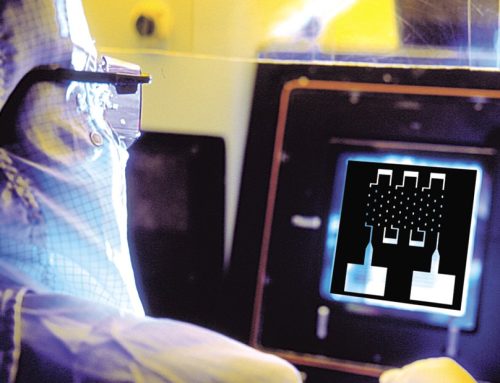
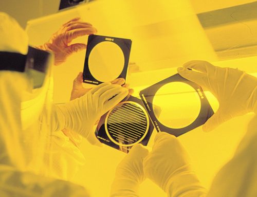
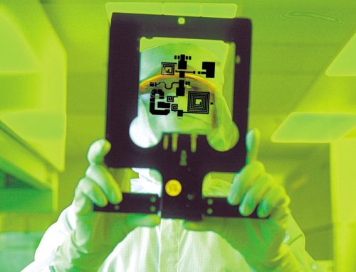
- Photomask: Term commonly used to describe the plate used in the photo litho process in the semiconductor/microelectronics industry. The image on the photomask is transferred to the substrate via a photographic process.
- Photo Resist: A photosensitive chemical, which is applied to the surface of the photomask substrate and into which the pattern data is written. Photo resist may be “positive” (exposed regions soften and are washed away during development) or “negative” (exposed regions are hardened and do not wash away during development).
- Pinhole: A clear area defect completely within a black (coated) pattern or in the black background (field).
- Plate: Photomasks are sometimes referred to as plates.
- Polarity: Indicates the tone of the data. Dark polarity would indicate clear patterns/dark background. Light polarity indicates dark patterns/light background. These terminologies are open for interpretation, and therefore terminologies that directly indicate the tone of either digitized (drawn) data, or non-digitized area (background) should be used whenever possible.
- Positive: A terminology sometimes used to define the tone of pattern features or background. Also referred to as light field or clear field. These terminologies are open for interpretation, and therefore terminologies that directly indicate the tone of either digitized (drawn) data, or non-digitized area (background) should be used whenever possible.
- Positive photo resist: A photosensitive resist that is decomposed (softened) by UV light and which, after exposure and development, is removed from those areas that were exposed.
- Process: In photomask terminology, process usually refers to the development of the image in the exposed photo resist coating on the photomask and the etching away of the underlying thin-film metal coating in the regions where the photo resist has been removed.
- Registration: The terminology used to explain how accurately the pattern features on a photomask overlay to another photomask in the same design set, or how the pattern overlays to a calibrated grid. A terminology used to explain positional accuracy of pattern features on the photomask.
- Resist: A photosensitive chemical, which is applied to the surface of the photomask substrate and into which the pattern data is written. Photo resist may be “positive” (exposed regions soften and are washed away during development) or “negative” (exposed regions are hardened and do not wash away during development). Also called photo resist.
- Resolution: A terminology used to define the smallest image that can be produced and subsequently processed on a photomask. Resolution varies from write tool to write tool.
- Reticle: A reticle is a photomask that is used in step and repeat exposure systems, called wafer steppers. Reticles may have only a single die, or an array of die, but do not contain sufficient pattern dice to cover a wafer unless used in a step & repeat system. Reticles are usually at a larger scale, such as 2X, 4X, 5X and 10X, but may also be at 1X.
- Right Reading Down (RRD), Right Reading Base (RRB): A photomask in which the functional pattern is shown with the coated surface of the photographic film or glass plate away from the viewer. The correct view of the pattern is seen while looking from the glass (base) side.
- Right Reading Up (RRU), Right Reading Emulsion (RRE): A photomask orientation in which the functional pattern is shown with the coated surface of the photographic film or glass plate toward the viewer. The correct view of the pattern is seen while looking from the coated side.
- Rotational error: The error that occurs when functional patterns are misaligned by some angle with respect to the X and Y axes during step-and-repeat.
- Semiconductor: A material wherein the conductive properties can be changed by temperature. Silicon, for example, acts as an insulator (non-conductive) when kept at low temperatures, but it becomes highly conductive when heated.
- Shadowmask: A thin sheet of metal produced using lithography, wherein the pattern is etched completely through the metal. The shadowmask is placed into intimate contact with the surface of a substrate, such as a silicon wafer. The shadowmask and the substrate are placed into a chemical vapor deposition (CVD) system and a thin-film coating, such as gold, is sputtered or evaporated through the shadowmask and onto the substrate. Also called a deposition mask.
- Soft Defects: Defects on a photomask that are of a temporary nature, such as dust, contamination and residual photo resist. Soft defects can usually be removed by re-cleaning the photomask.
- Step & Repeat: A method of dimensionally positioning multiples of the same or intermixed functional patterns accurately within a given area on a photoplate or a film by repetitious contact or projection printing.
- Stepper: A lithography system that exposes a substrate by projecting an image on a reticle multiple times at various X, Y coordinates. In many cases the optics in the stepper reduce the reticle pattern to achieve a 1X substrate.
- Substrate: The base material on which the photomask is made (quartz or soda lime glass). This terminology may also used to describe the base material onto which the photomask pattern will be transferred such as silicon wafers, glass or metal.
- Test pattern: A pattern used for inspection or testing purposes.
- Wafer: A thin substrate material, usually silicon, upon which an Integrated circuit is created through a process of multiple lithography steps, each using a unique photomask pattern. Each lithography step usually includes deposition of a thin film material (metal, glass, etc.), application of a thin coating of photo resist, exposure using a photomask, develop, etch, strip & clean.
- Write: The process wherein a photo resist coating is sensitized by an energy source (UV, e-beam, laser, etc.), for the purpose of exposing certain regions and leaving other regions unexposed.
- X axis: The horizontal or left-to-right directions in a two-dimensional system of coordinates.
- Y-axis: The vertical direction, perpendicular to the X-axis, in a two-dimensional system of coordinates.

